| The subject of this article is from the Origins update.
The information from this article is up-to-date as of 9 November, 2020. |
The information from this article is up-to-date as of 9 November, 2020.
Combinational Circuits is a power-related page.
Summary[ | ]
This page is dedicated to circuits that have their outputs as a function of their inputs. These circuits have many uses in checking whether certain conditions are met, as well as being a fundamental part of more complex circuits such as memory circuits.
A stable circuit is defined as having its input be unaffected from its output and each input be unaffected by another. Unstable circuits should only be used in isolation as power can flow from output to input and ruin the circuit.
Logic Gates[ | ]
Two-input logic gates have their inputs labeled A and B, single-input gates have their input labeled P, and outputs are labeled Q. An input labeled "1" indicates that constant power must be supplied to it.
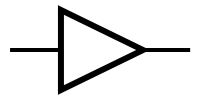
Buffer Gate[ | ]
Buffer Gate Symbol
| P | Q | |
|---|---|---|
| 0 | 0 | |
| 1 | 1 |
A buffer gate is a single-input logic gate that simply outputs power when the input is on. This is also called a diode because it only allows information to travel in one direction, which is used to make a circuit stable.
| Name | Description | Stable | Materials | Diagram | Image |
|---|---|---|---|---|---|
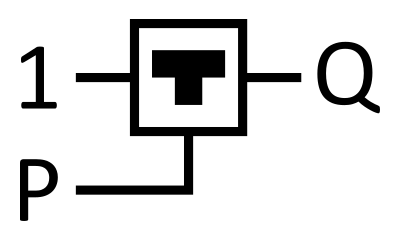
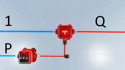
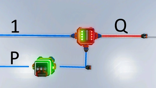
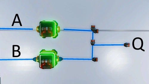
| Design A | A single Auto Switch supplied with constant power will output power only if the middle input is on. This design also functions as a diode, only allowing for output Q to be altered by input P and preventing P from being altered by Q. | Yes |
|
 |
 |
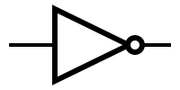
NOT Gate[ | ]

NOT Gate Symbol
| P | Q | |
|---|---|---|
| 0 | 1 | |
| 1 | 0 |
A NOT gate is a single-input logic gate that negates the input, outputting power only if the input is off.
| Name | Description | Stable | Materials | Diagram | Image |
|---|---|---|---|---|---|
| Design A | A single Power Inverter supplied with constant power will output power only if the middle output is off, thereby acting as a negation of the middle input. | Yes | 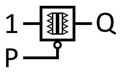 |
 |
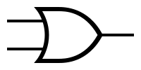
OR Gate[ | ]

OR Gate Symbol
| A | B | Q | |
|---|---|---|---|
| 0 | 0 | 0 | |
| 0 | 1 | 1 | |
| 1 | 0 | 1 | |
| 1 | 1 | 1 |
An OR gate is a multiple-input logic gate that outputs power only if at least one input is on.
| Name | Description | Stable | Materials | Diagram | Image |
|---|---|---|---|---|---|
| Design A | Connecting two pieces of Electrical Wiring together acts as a simple OR gate, however power can flow through both directions. | No | N/A | 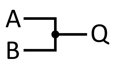 |
 |
| Design B | Design 3B but with 2 inputs | Yes |
|
 |
 |
| Design 3A | Design A can extend to any number of inputs | No | N/A |  |
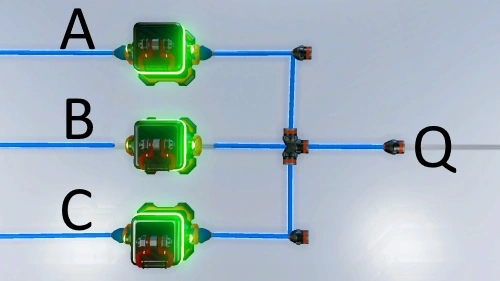 |
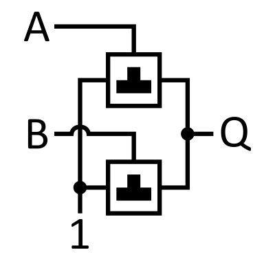
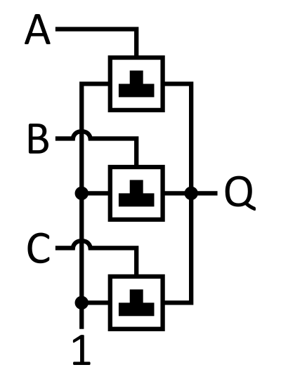
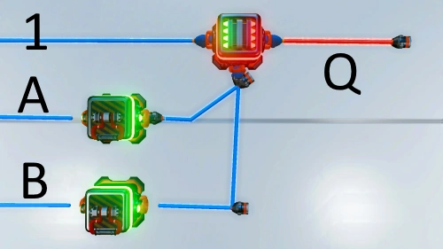
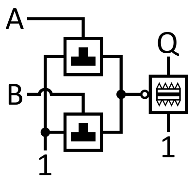
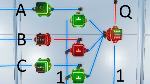
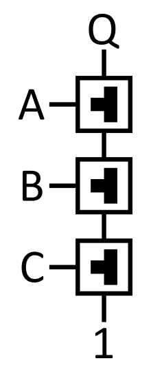
| Design 3B[1] | This design has a 3-input OR gate, but the number of inputs can be increased. This circuit is fundamentally a combination of 3 buffer gates and using design 3A to OR their outputs together. See also: OR Gate |
Yes |
|
 |
 |
NOR Gate[ | ]

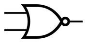
NOR Gate Symbol
| A | B | Q | |
|---|---|---|---|
| 0 | 0 | 1 | |
| 0 | 1 | 0 | |
| 1 | 0 | 0 | |
| 1 | 1 | 0 |
A NOR gate is the negation of an OR gate. It is a multiple-input logic gate that outputs power only if no input is on.
| Name | Description | Stable | Materials | Diagram | Image |
|---|---|---|---|---|---|
| Design A | By connecting both inputs to the middle input of the power inverter, it acts as OR gate design A before being negated using NOT gate design A. | No | 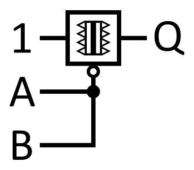 |
 | |
| Design B | Created by connecting OR gate design B to a NOT gate | Yes |
|
 |
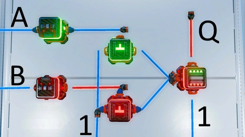 |
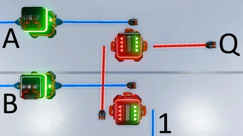
| Design C | By connecting the output of one power inverter to the input of another, the circuit acts as an AND of the negation of all inputs, which is logically equivalent to a NOR of all inputs. | Yes | 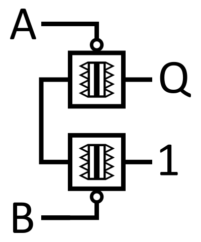 |
 | |
| Design 3A | Created by extending OR gate design A to 3 inputs and connecting it to a NOT gate | No | 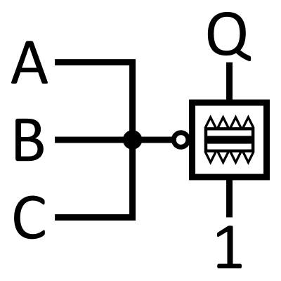 |
 | |
| Design 3B | Created by connecting OR gate design 3B to a NOT gate | Yes |
|
 |
 |
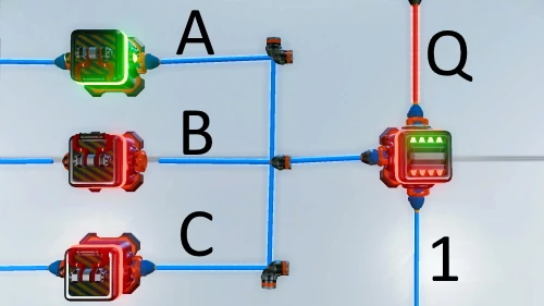
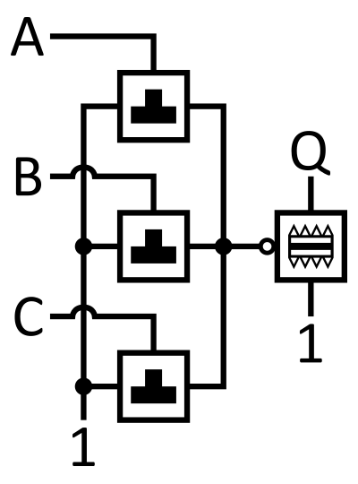
| Design 3C | Created by extending design C to 3 inputs. Delay increases with number of inputs, but requires less components than 3B. | Yes | 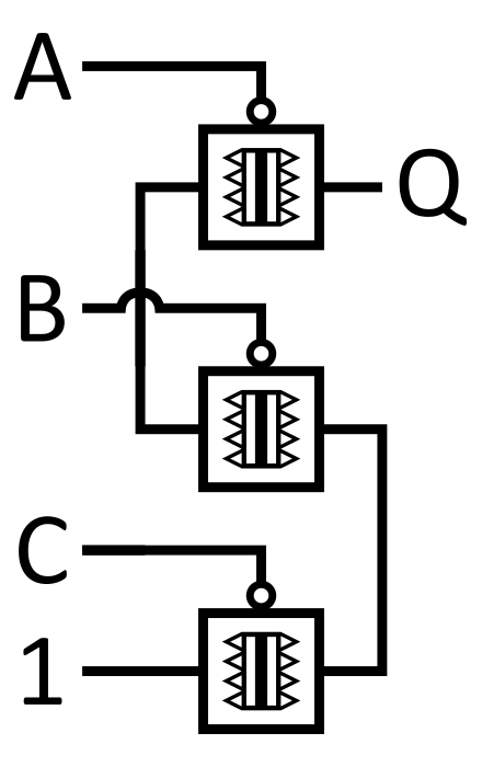 |
 |
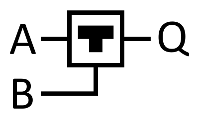
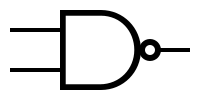
AND Gate[ | ]

AND Gate Symbol
| A | B | Q | |
|---|---|---|---|
| 0 | 0 | 0 | |
| 0 | 1 | 0 | |
| 1 | 0 | 0 | |
| 1 | 1 | 1 |
An AND gate is a multiple-input logic gate that outputs power only if all inputs are on.
| Name | Description | Stable | Materials | Diagram | Image |
|---|---|---|---|---|---|
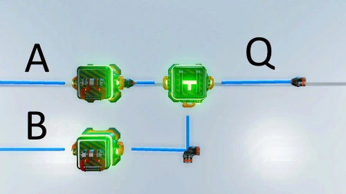
| Design A | A single Auto Switch acts as an AND gate when treating the power input as input A and the control input as input B. See also: Basic_Circuits#Components |
No |
|
 |
 |
| Design B | Design 3B but with 2 inputs | Yes |
|
 |
 |
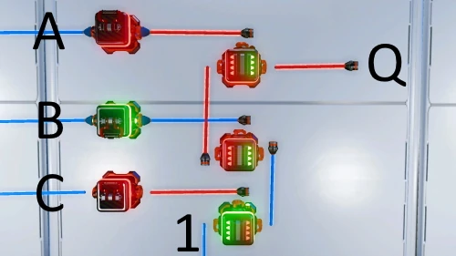
| Design 3B[1] | This design has a 3-input AND gate, but the number of inputs can be increased by adding more Auto Switches. As the output of one feeds the next, only when all three (or as many as you want) auto switches have power will the final output be powered. See also: AND gate |
Yes |
|
 |
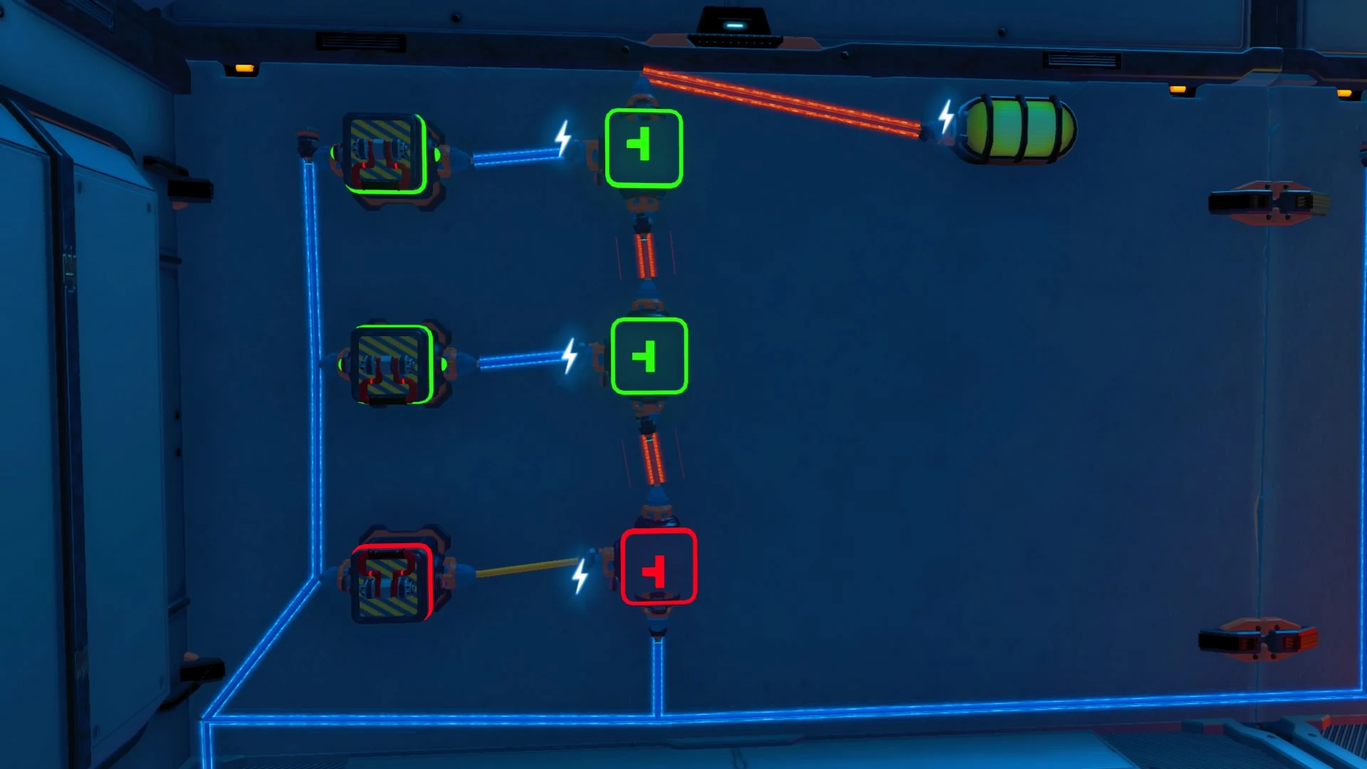 |
NAND Gate[ | ]

NAND Gate Symbol
| A | B | Q | |
|---|---|---|---|
| 0 | 0 | 1 | |
| 0 | 1 | 1 | |
| 1 | 0 | 1 | |
| 1 | 1 | 0 |
A NAND gate is the negation of an AND gate. It is a multiple-input logic gate that outputs power only if not all inputs are on.
| Name | Description | Stable | Materials | Diagram | Image |
|---|---|---|---|---|---|
| Design A | Created by connecting AND gate design A to NOT gate design A | Yes |
|
 |
 |
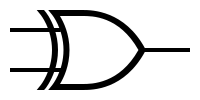
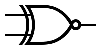
XOR Gate[ | ]
XOR Gate Symbol
| A | B | Q | |
|---|---|---|---|
| 0 | 0 | 0 | |
| 0 | 1 | 1 | |
| 1 | 0 | 1 | |
| 1 | 1 | 0 |
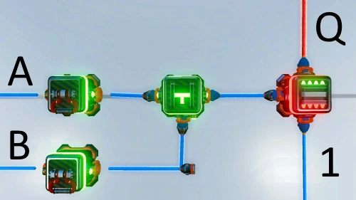
An XOR gate is a two-input logic gate that outputs power only if either input is on, but not both. In other words, if the two inputs are different.
| Name | Description | Stable | Materials | Diagram | Image |
|---|---|---|---|---|---|
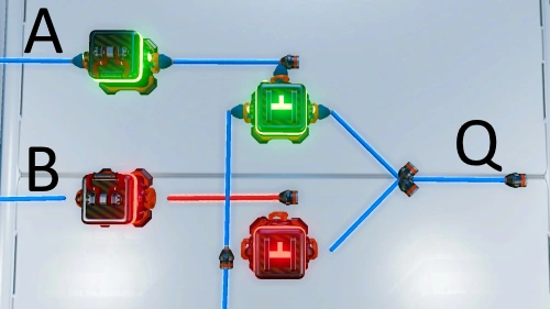
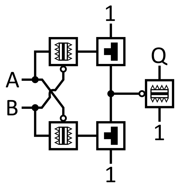
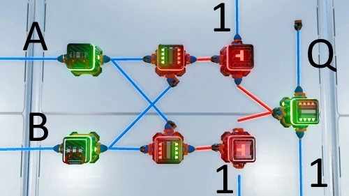
| Design A[2] | Based on the logical expression "(A AND (NOT B)) OR ((NOT A) AND B)", equivalent to "(A NIMPLY B) OR (B NIMPLY A)". Created using NIMPLY gate design A and OR gate design A, with the outputs connected to diodes. | Yes |
|
 |
 |
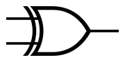
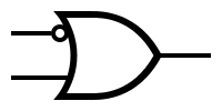
XNOR Gate[ | ]

XNOR Gate Symbol
| A | B | Q | |
|---|---|---|---|
| 0 | 0 | 1 | |
| 0 | 1 | 0 | |
| 1 | 0 | 0 | |
| 1 | 1 | 1 |
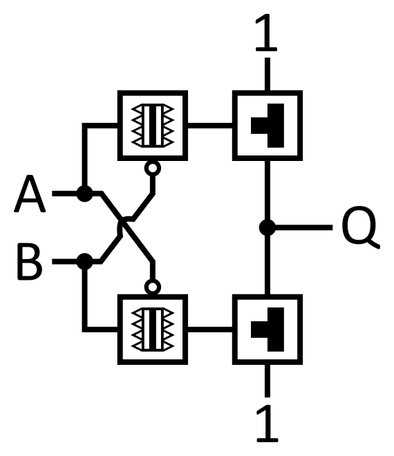
An XNOR gate is the negation of an XOR gate. It is a two-input logic gate that outputs power only if either both or no inputs are on. In other words, if the two inputs are the same.
| Name | Description | Stable | Materials | Diagram | Image |
|---|---|---|---|---|---|
| Design A | Created by connecting XOR gate design A to NOT gate design A. | Yes |
|
 |
 |
IMPLY Gate[ | ]

IMPLY Gate Symbol
| A | B | Q | |
|---|---|---|---|
| 0 | 0 | 1 | |
| 0 | 1 | 1 | |
| 1 | 0 | 0 | |
| 1 | 1 | 1 |
An IMPLY gate is a two-input logic gate that outputs power only if the logical IMPLY operation between the inputs is true. It will not output power when input A is true and input B is false, otherwise it will output power. This is equivalent to "(NOT A) OR B".
| Name | Description | Stable | Materials | Diagram | Image |
|---|---|---|---|---|---|
| Design A | Created by connecting NIMPLY gate design A to NOT gate design A. | Yes | 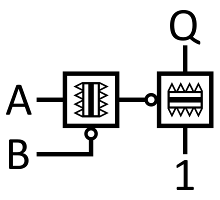 |
 |
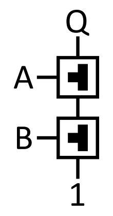
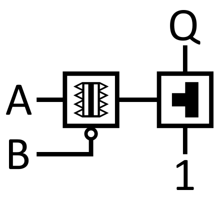
NIMPLY Gate[ | ]

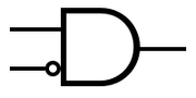
NIMPLY Gate Symbol
| A | B | Q | |
|---|---|---|---|
| 0 | 0 | 0 | |
| 0 | 1 | 0 | |
| 1 | 0 | 1 | |
| 1 | 1 | 0 |
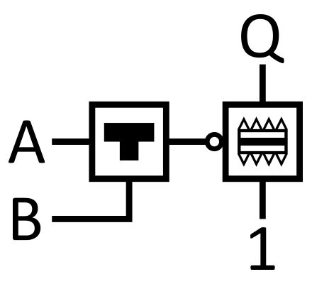
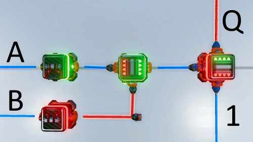
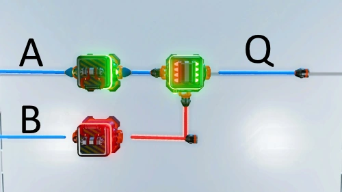
A NIMPLY gate is the negation of an IMPLY gate. It is a two-input logic gate that outputs power only if the logical IMPLY operation between the inputs is false. It will only output power when input A is true and input B is false. This is equivalent to "A AND (NOT B)".
| Name | Description | Stable | Materials | Diagram | Image |
|---|---|---|---|---|---|
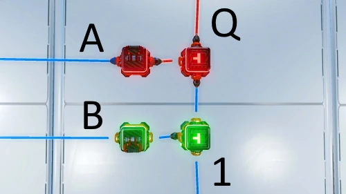
| Design A | A single Power Inverter acts as a NIMPLY gate when treating the power input as input A and the control input as input B. See also: Basic_Circuits#Components |
No |  |
 | |
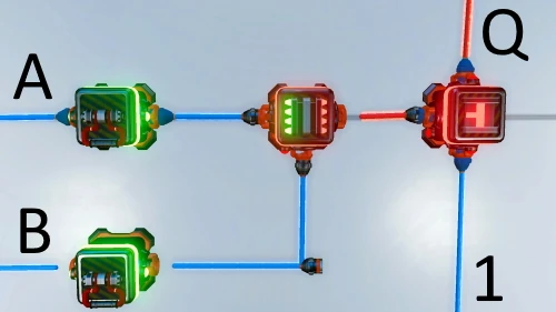
| Design B | Created by connecting design A to a diode. | Yes |
|
 |
 |
Multiplexers And Demultiplexers[ | ]
Multiplexer[ | ]
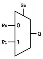
2-Input Multiplexer Symbol
| S0 | S1 | Q | |
|---|---|---|---|
| 0 | 0 | P0 | |
| 0 | 1 | P1 | |
| 1 | 0 | P2 | |
| 1 | 1 | P3 |
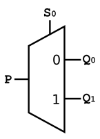
| S0 | Q | |
|---|---|---|
| 0 | P0 | |
| 1 | P1 |
A multiplexer (mux, for short) is used to select a single signal from multiple inputs and send it to a single output. Multiplexers typically have 2^N inputs and N "selector" inputs which determine the signal to use. For example, a 2-input mux would have 2 inputs and 1 selector signal, a 4-input mux would have 4 inputs and 2 selectors, an 8-input would have 8 and 3, etc. On this page, the inputs are labeled "P0", "P1", etc., the selector inputs are labeled "S0", "S1", etc., and the output is labeled Q. The selectors are chosen such that it would be like counting in binary, e.g. S0 and S1 being off would correspond to choosing P0 and S0 and S1 being on would correspond to choosing P1.
Each design name is prefixed with the number of inputs.
| Name | Description | Stable | Materials | Diagram | Image |
|---|---|---|---|---|---|
| Design 2A | Design 4A but with 2 inputs and 1 selector | Yes |
|
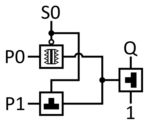 |
 |
| Design 4A[1] | A 2x4 grid of Auto Switches and Power Inverters is arranged so that the left input is the circuit's specified input and the control signal comes from the corresponding selector signal, all being ORed together and fed into a diode. | Yes |
|
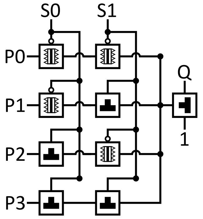 |
 |
Demultiplexer[ | ]
2-Output Demultiplexer Symbol
| S0 | S1 | Q0 | Q1 | Q2 | Q3 | |
|---|---|---|---|---|---|---|
| 0 | 0 | P | 0 | 0 | 0 | |
| 0 | 1 | 0 | P | 0 | 0 | |
| 1 | 0 | 0 | 0 | P | 0 | |
| 1 | 1 | 0 | 0 | 0 | P |
| S0 | Q0 | Q1 | |
|---|---|---|---|
| 0 | P | 0 | |
| 1 | 0 | P |
A demultiplexer (demux, for short) is used to select a specified output path for a single input. Demultiplexers typically have 2^N outputs and N selector inputs which determine which output will be chosen. This circuit is the inverse of the Multiplexer. On this page, the single input is labeled P, the selectors are labeled "S0", "S1", etc., and the outputs are labeled "Q0", "Q1", etc. The selectors are chosen such that it would be like counting in binary, e.g. S0 and S1 being off would correspond to output Q0 taking the value of P and all others remaining off.
Each design name is prefixed with the number of outputs.
| Name | Description | Stable | Materials | Diagram | Image |
|---|---|---|---|---|---|
| Design 2A | Design 4A but with 2 outputs and 1 selector | Yes |
|
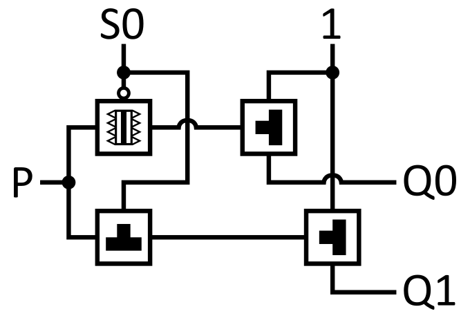 |
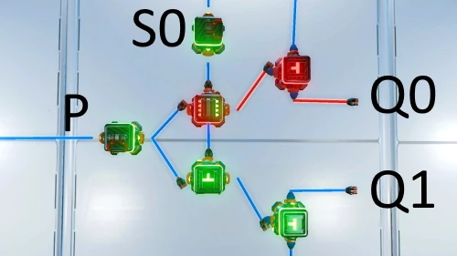 |
| Design 4A[1] | A 2x4 grid of Auto Switches and Power Inverters is arranged so that the left input is the circuit's input and the control signal comes from the corresponding selector signal. Then he output from each final component is sent to the different outputs, each prefixed with a diode. | Yes |
|
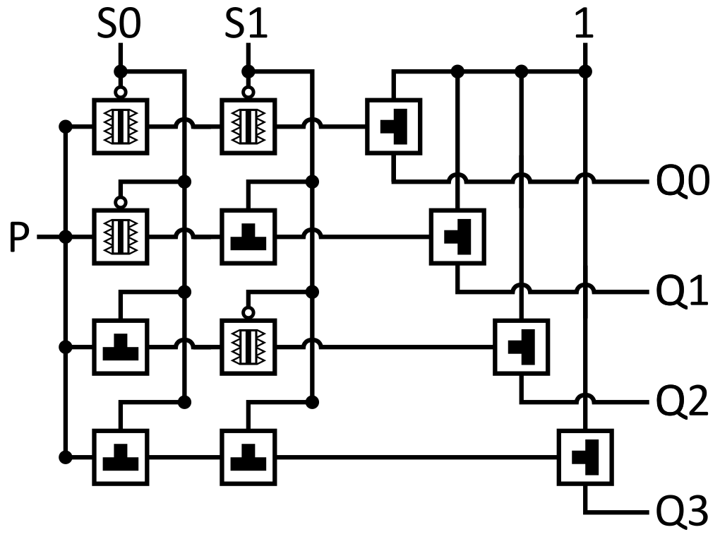 |
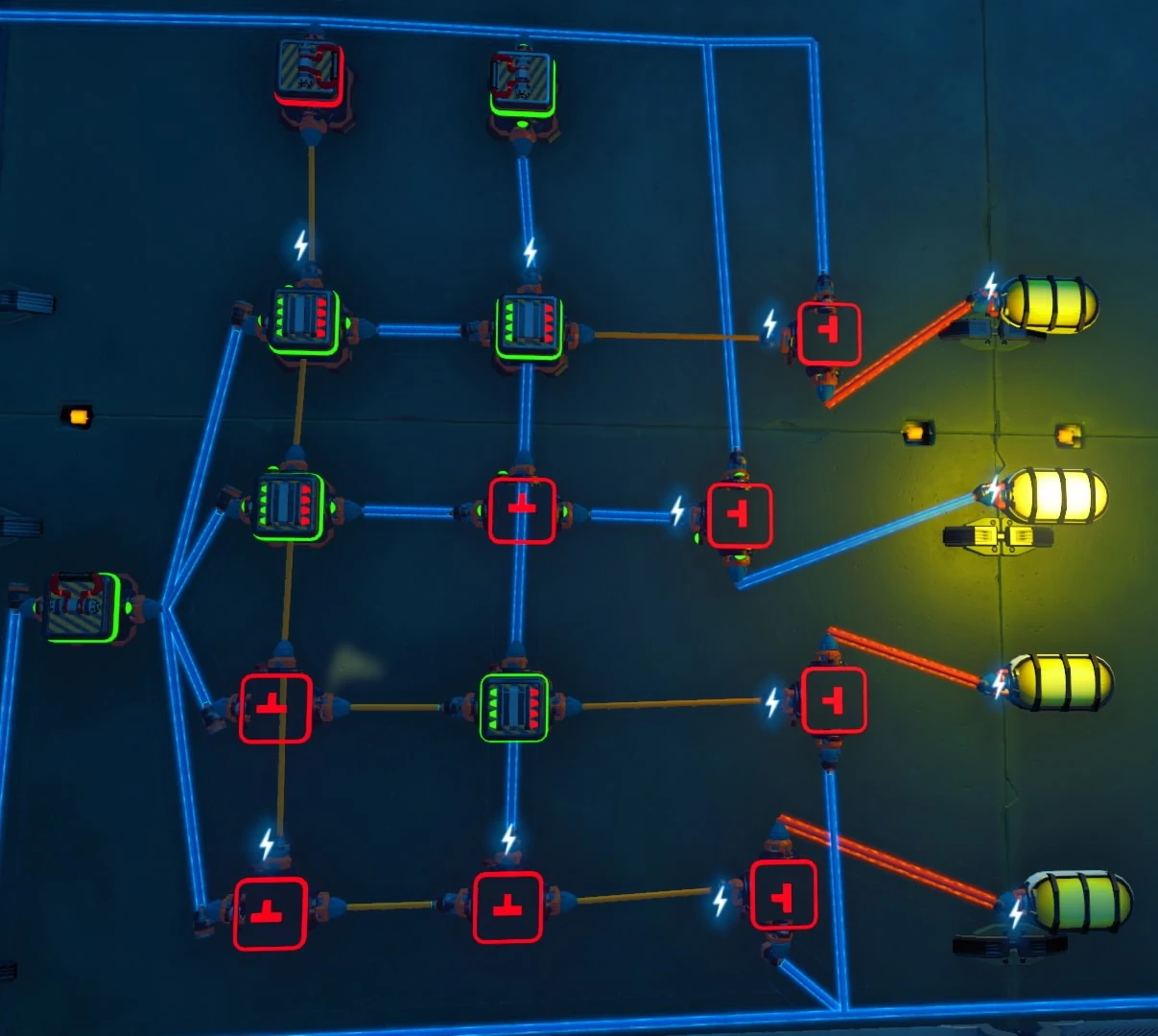 |
References[ | ]
- ↑ 1.0 1.1 1.2 1.3 /u/Achereto "No Man's Logic 2: Improved gates and building blocks"
- ↑ /u/Achereto "No Man's Logic."